Diodes 1N4001G - 1N4007G Manuel d'utilisateur

Naviguer en ligne ou télécharger Manuel d'utilisateur pour Matériel Diodes 1N4001G - 1N4007G. Diodes 1N4001G - 1N4007G User Manual Manuel d'utilisatio

  • Télécharger
  • Ajouter à mon manuel
  • Imprimer
  • Page
    / 3
  • Table des matières
  • MARQUE LIVRES
  • Noté. / 5. Basé sur avis des utilisateurs
Vue de la page 0
1N4001G – 1N4007G
Document number: DS29002 Rev. 8 - 2
1 of 3
www.diodes.com
January 2012
© Diodes Incorporated
1N4001G - 1N4007G
1.0A GLASS PASSIVATED RECTIFIER
Features and Benefits
Glass Passivated Die Construction
High Current Capability and Low Forward Voltage Drop
Surge Overload Rating to 30A Peak
Lead Free Finish, RoHS Compliant (Note 1)
Mechanical Data
Case: DO-41 Plastic
Case Material: Molded Plastic. UL Flammability Classification
Rating 94V-0
Moisture Sensitivity: Level 1 per J-STD-020
Terminals: Finish - Tin. Plated Leads Solderable per MIL-STD-
202, Method 208
Polarity: Cathode Band
Marking: Type Number
Weight: 0.30 grams (approximate)
Ordering Information (Note 2)
Device Packaging Shipping
1N4001G-T DO-41 Plastic 5K/Tape & Reel, 13-inch
1N4002G-T DO-41 Plastic 5K/Tape & Reel, 13-inch
1N4003G-T DO-41 Plastic 5K/Tape & Reel, 13-inch
1N4004G-T DO-41 Plastic 5K/Tape & Reel, 13-inch
1N4005G-T DO-41 Plastic 5K/Tape & Reel, 13-inch
1N4006G-T DO-41 Plastic 5K/Tape & Reel, 13-inch
1N4007G-T DO-41 Plastic 5K/Tape & Reel, 13-inch
Maximum Ratings and Electrical Characteristics @T
A
= 25°C unless otherwise specified
Single phase, half wave, 60Hz, resistive or inductive load.
For capacitive load, derate current by 20%.
Characteristic Symbol
1N4001
G
1N4002
G
1N4003
G
1N4004
G
1N4005
G
1N4006
G
1N4007
G
Unit
Peak Repetitive Reverse Voltage
Working Peak Reverse Voltage
DC Blocking Voltage
V
RRM
V
RWM
V
R
50 100 200 400 600 800 1000 V
RMS Reverse Voltage
V
R
(
RMS
)
35 70 140 280 420 560 700 V
Average Rectified Output Current (Note 3) @ T
A
= 75°C I
O
1.0 A
Non-Repetitive Peak Forward Surge Current 8.3ms
single half sine-wave superimposed on rated load
I
FSM
30 A
Forward Voltage @ I
F
= 1.0A V
FM
1.0 V
Peak Reverse Current @T
A
= 25°C
at Rated DC Blocking Voltage @ T
A
= 125°C
I
RM
5.0
50
µA
Typical Reverse Recovery Time (Note 4)
t
r
r
2.0 µs
Typical Total Capacitance (Note 5)
C
T
8.0 pF
Typical Thermal Resistance Junction to Ambient
R
θ
JA
100 °C/W
Operating and Storage Temperature Range
T
J
,
T
STG
-65 to +175 °C
Notes: 1. EU Directive 2002/95/EC (RoHS). All applicable RoHS exemptions applied, see EU Directive 2002/95/EC Annex Notes.
2. For packaging details, visit our website at http://www.diodes.com.
3. Leads maintained at ambient temperature at a distance of 9.5mm from the case.
4. Measured with I
F
= 0.5A, I
R
= -1A, I
rr
= 0.25A.
5. Measured at 1.0 MHz and applied reverse voltage of 4.0V DC.
Vue de la page 0
1 2 3

Résumé du contenu

Page 1 - 1N4001G – 1N4007G

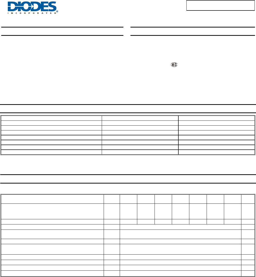
1N4001G – 1N4007G Document number: DS29002 Rev. 8 - 2 1 of 3 www.diodes.com January 2012© Diodes Incorporated 1N4001G - 1N4007G 1.0A GLASS PASSIVA

Page 2 - 1N4001G - 1N4007G

1N4001G – 1N4007G Document number: DS29002 Rev. 8 - 2 2 of 3 www.diodes.com January 2012© Diodes Incorporated 1N4001G - 1N4007G 4060 80100120140

Page 3 - Package Outline Dimensions

1N4001G – 1N4007G Document number: DS29002 Rev. 8 - 2 3 of 3 www.diodes.com January 2012© Diodes Incorporated 1N4001G - 1N4007G Package Outlin

Commentaires sur ces manuels

Pas de commentaire