Diodes DCP68/-25 Manuel d'utilisateur
Naviguer en ligne ou télécharger Manuel d'utilisateur pour Matériel Diodes DCP68/-25. Diodes DCP68/-25 User Manual Manuel d'utilisatio
- Page / 4
- Table des matières
- MARQUE LIVRES
Résumé du contenu
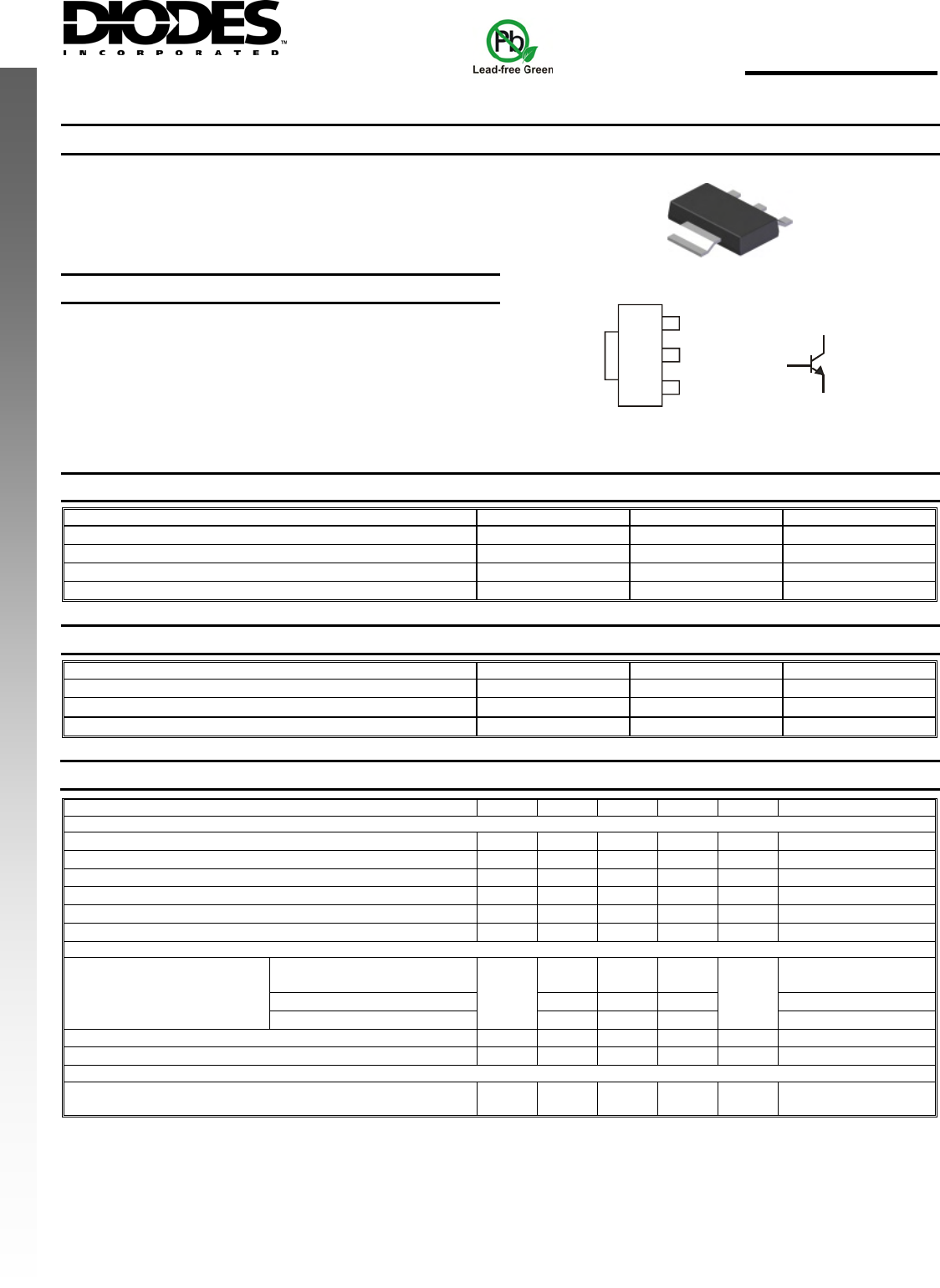
DS30797 Rev. 6 - 2 1 of 4 www.diodes.com DCP68/-25 © Diodes Incorporated DCP68/-25 NPN SURFACE MOUNT TRANSISTOR Features • Epitaxial Planar Di
DS30797 Rev. 6 - 2 2 of 4 www.diodes.com DCP68/-25 © Diodes Incorporated V , COLLECTOR EMITTER VOLTAGE (V)CEI, COLLECTOR CURRENT (A)C0.00.20.4
DS30797 Rev. 6 - 2 3 of 4 www.diodes.com DCP68/-25 © Diodes Incorporated CAPACITANCE (pF)V , REVERSE VOLTAGE (V)R1101000.1 1 10 100 Fig. 8 Typ
DS30797 Rev. 6 - 2 4 of 4 www.diodes.com DCP68/-25 © Diodes Incorporated Suggested Pad Layout: (Unit: mm) NEW PRODUCT IM
Produits connexes et manuels pour Matériel Diodes DCP68/-25
 (5 pages)
© 2020, manymanuals.fr. Tous droits réservés | 0.618 s |
 Manymanuals.com
 Manymanuals.de
 Manymanuals.fr
 Manymanuals.it
 Manymanuals.pl
 Manymanuals.cz
 Manymanuals.es
 Manymanuals-pt.com
Commentaires sur ces manuels