2N7002VC/VAC
Document number: DS30639 Rev. 6 - 2
2 of 4
www.diodes.com
October 2011
© Diodes Incorporated
2N7002VC/VAC
NEW PRODUCT
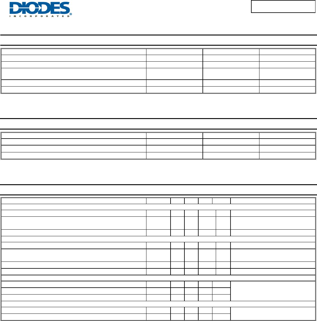
Maximum Ratings @T
A
= 25°C unless otherwise specified
Characteristic Symbol Value Units
Drain-Source Voltage
V
DSS
60 V
Drain-Gate Voltage R
GS
≤ 1.0MΩ V
DGR
60 V
Gate-Source Voltage (Note 5) Continuous
Pulsed
V
GSS
±20
±40
V
Drain Current (Note 5) Continuous
I
D
280 mA
Drain Current (Note 5) Pulsed
I
DM
1.5 A
Thermal Characteristics @T
A
= 25°C unless otherwise specified
Characteristic Symbol Value Units
Total Power Dissipation
P
D
150 mW
Thermal Resistance, Junction to Ambient
R
JA
833 °C/W
Operating and Storage Temperature Range
T
J,
T
STG
-55 to +150 °C
Electrical Characteristics @T
A
= 25°C unless otherwise specified
Characteristic Symbol Min Typ Max Unit Test Condition
OFF CHARACTERISTICS (Note 6)
Drain-Source Breakdown Voltage
BV
DSS
60 70
⎯
V
V
GS
= 0V, I
D
= 10μA
Zero Gate Voltage Drain Current @ T
C
= 25°C
@ T
C
= 125°C
I
DSS
⎯ ⎯
1.0
500
µA
V
DS
= 60V,
V
GS
= 0V
Gate-Body Leakage
I
GSS
⎯ ⎯
±100 nA
V
GS
= ±20V, V
DS
= 0V
ON CHARACTERISTIC (Note 6)
Gate Threshold Voltage
V
GS
th
1.0
⎯
2.5 V
V
DS
= V
GS
, I
D
= 250μA
Static Drain-Source On-Resistance
R
DS (ON)
⎯
⎯
⎯
⎯
7.5
13.5
Ω
V
GS
= 5V, I
D
= 0.05A,
V
GS
= 10V, I
D
= 0.5A, T
= 125°C
On-State Drain Current
I
D
ON
0.5 1.0
⎯
A
V
GS
= 10V,
V
DS
= 7.5V
Forward Transconductance
g
FS
80
⎯ ⎯
mS
V
DS
= 10V, I
D
= 0.2A
DYNAMIC CHARACTERISTICS
Input Capacitance
C
iss
⎯ ⎯
50 pF
V
DS
= 25V, V
GS
= 0V, f = 1.0MHz
Output Capacitance
C
oss
⎯ ⎯
25 pF
Reverse Transfer Capacitance
C
rss
⎯ ⎯
5.0 pF
SWITCHING CHARACTERISTICS
Turn-On Delay Time
t
D
ON
⎯ ⎯
20 ns
V
DD
= 30V, I
D
= 0.2A, R
L
= 150Ω,
V
GEN
= 10V, R
GEN
= 25Ω Turn-Off Delay Time
t
D
OFF
⎯ ⎯
20 ns
Notes: 5. Device mounted on FR-4 PCB, 1 inch x 0.85 inch x 0.062 inch; pad layout as shown on Diodes Inc. suggested pad layout document AP02001, which can
be found on our website at http://www.diodes.com.
6. Short duration pulse test used to minimize self-heating effect.
 (1 pages)
 Manymanuals.com
 Manymanuals.de
 Manymanuals.fr
 Manymanuals.it
 Manymanuals.pl
 Manymanuals.cz
 Manymanuals.es
 Manymanuals-pt.com
Commentaires sur ces manuels