Diodes 2DB1714 Manuel d'utilisateur

Naviguer en ligne ou télécharger Manuel d'utilisateur pour Matériel Diodes 2DB1714. Diodes 2DB1714 User Manual [fr] Manuel d'utilisatio

  • Télécharger
  • Ajouter à mon manuel
  • Imprimer
  • Page
    / 4
  • Table des matières
  • MARQUE LIVRES
  • Noté. / 5. Basé sur avis des utilisateurs
Vue de la page 0
2DB1714
Document number: DS31610 Rev. 2 - 2
1 of 4
www.diodes.com
December 2008
© Diodes Incorporated
2DB1714
NEW PRODUCT
LOW V
CE(SAT)
PNP SURFACE MOUNT TRANSISTOR
Features
Epitaxial Planar Die Construction
Ideally Suited for Automated Assembly Processes
Ideal for Medium Power Switching or Amplification Applications
Complementary NPN Type (2DD2679) Available
Lead Free By Design/RoHS Compliant (Note 1)
"Green" Device (Note 2)
Mechanical Data
Case: SOT89-3L
Case Material: Molded Plastic, "Green” Molding Compound.
UL Flammability Classification Rating 94V-0
Moisture Sensitivity: Level 1 per J-STD-020D
Terminals: Finish — Matte Tin annealed over Copper leadframe
(Lead Free Plating). Solderable per MIL-STD-202, Method 208
Marking Information: See Page 4
Ordering Information: See Page 4
Weight: 0.072 grams (approximate)
Maximum Ratings @T
A
= 25°C unless otherwise specified
Characteristic Symbol Value Unit
Collector-Base Voltage
V
CBO
-30 V
Collector-Emitter Voltage
V
CEO
-30 V
Emitter-Base Voltage
V
EBO
-6 V
Peak Pulse Current
I
CM
-4 A
Continuous Collector Current
I
C
-2 A
Thermal Characteristics
Characteristic Symbol Value Unit
Power Dissipation (Note 3) @ T
A
= 25°C P
D
0.9 W
Thermal Resistance, Junction to Ambient Air (Note 3) @ T
A
= 25°C
R
θ
JA
139 °C/W
Power Dissipation (Note 4) @ T
A
= 25°C P
D
2 W
Thermal Resistance, Junction to Ambient Air (Note 4) @ T
A
= 25°C
R
θ
JA
62.5 °C/W
Operating and Storage Temperature Range
T
J
, T
STG
-55 to +150 °C
Electrical Characteristics @T
A
= 25°C unless otherwise specified
Characteristic Symbol Min Typ Max Unit Conditions
OFF CHARACTERISTICS
Collector-Base Breakdown Voltage
V
(
BR
)
CBO
-30
V
I
C
= -10μA, I
E
= 0
Collector-Emitter Breakdown Voltage (Note 5)
V
(
BR
)
CEO
-30
V
I
C
= -1mA, I
B
= 0
Emitter-Base Breakdown Voltage
V
(
BR
)
EBO
-6
V
I
E
= -10μA, I
C
= 0
Collector Cut-Off Current
I
CBO
-0.1
μA
V
CB
= -30V, I
E
= 0
Emitter Cut-Off Current
I
EBO
-0.1
μA
V
EB
= -6V, I
C
= 0
ON CHARACTERISTICS (Note 5)
Collector-Emitter Saturation Voltage
V
CE
(
SAT
)
-370 mV
I
C
= -1.5A, I
B
= -75mA
DC Current Gain
h
FE
270
680
V
CE
= -2V, I
C
= -200mA
SMALL SIGNAL CHARACTERISTICS
Output Capacitance
C
obo
16
pF
V
CB
= -10V, I
E
= 0,
f = 1MHz
Current Gain-Bandwidth Product
f
T
200
MHz
V
CE
= -2V, I
C
= -100mA,
f = 100MHz
Notes: 1. No purposefully added lead.
2. Diodes Inc.'s "Green" policy can be found on our website at http://www.diodes.com/products/lead_free/index.php.
3. Device mounted on FR-4 PCB with minimum recommended pad layout.
4. Device mounted on FR-4 PCB with 1 inch
2
copper pad layout.
5. Measured under pulsed conditions. Pulse width = 300μs. Duty cycle 2%.
Top View
Device Schematic
Pin Out Configuration
3
1
2,4
C
O
L
L
E
C
T
O
R
E
M
I
T
T
E
R
B
A
S
E
4
3
2
1
C
C
B
E
T
O
P
V
I
E
W
Please click here to visit our online spice models database.
Vue de la page 0
1 2 3 4

Résumé du contenu

Page 1

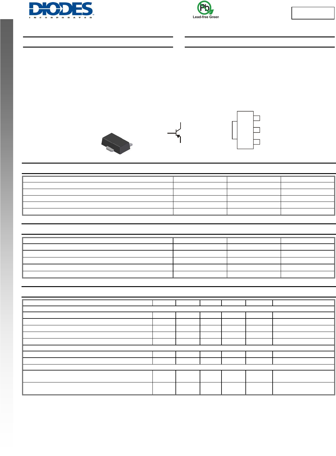
2DB1714 Document number: DS31610 Rev. 2 - 2 1 of 4 www.diodes.com December 2008© Diodes Incorporated 2DB1714NEW PRODUCT LOW VCE(SAT) PNP SURFACE

Page 2 - NEW PRODUCT

2DB1714 Document number: DS31610 Rev. 2 - 2 2 of 4 www.diodes.com December 2008© Diodes Incorporated 2DB1714NEW PRODUCT 00.40.825 5075100 12515

Page 3

2DB1714 Document number: DS31610 Rev. 2 - 2 3 of 4 www.diodes.com December 2008© Diodes Incorporated 2DB1714NEW PRODUCT 1 10 100 1,000 10,000-I

Page 4 - © Diodes Incorporated

2DB1714 Document number: DS31610 Rev. 2 - 2 4 of 4 www.diodes.com December 2008© Diodes Incorporated 2DB1714NEW PRODUCT Ordering Information (N

Commentaires sur ces manuels

Pas de commentaire